Abstract: In recent years, the application of high-power semiconductor lasers has been expanding, and they are more and more widely used in industry and medical treatment. The thermal characteristics of lasers seriously restrict their reliability and service life. In order to improve the reliability and prolong the service life of the device,high power semiconductor laser bars with different solders, different thickness of solders and different thickness of WCu heat sink packages were simulated by COMSOL Multiphysics, and the “Smile” values of laser bars under different packaging conditions were measured. The results show that the maximum thermal stress of in solder or AuSn solder occurs at the interface between WCu secondary heat sink and Cu heat sink; the thermal stress of laser chips packaged with the same thickness of In solder and AuSn solder is 3.57 GPa and 3.83 GPa respectively,and the peak spectra are 800.5 and 798 nm, respectively.; reducing the thickness of solder is beneficial to reducing the thermal stress and temperature in the laser chips,but the solder is not. If the thickness is too thin,it may lead to weak welding of the laser core or uneven distribution of solder,and voids in the solder layer,so the selection of solder thickness should be considered as a whole. With the increase of the thickness of WCu secondary heat sink, the thermal stress of the laser chip decreases,but the temperature of the core rises,and the optimal thickness of tungsten-copper secondary heat sink is 380 um. This paper provides a basis for optimizing the packaging of high power semiconductor lasers and has guiding significance for practical production.
- Introduction
With its small size, light weight, high efficiency and easy modulation, high-power semiconductor lasers are widely used in materials processing, medical and cosmetic, military and defense [1]-[6]. At present, high-power semiconductor lasers that operate continuously at room temperature have a maximum electro-optic conversion efficiency of approximately 70% [7], so a large amount of waste heat will be generated during operation. If the excess heat is not released in time, the temperature of the laser die will rise, resulting in a change in the forbidden band width of the material, which seriously affects the stability of the output beam. In addition, because the thermal expansion coefficient between the laser die and the heat sink material does not match, the temperature change will cause thermal stress to occur, and the output spectrum will change. If the thermal stress is too large, the bonding layer will be cracked. Problems such as die breakage have seriously affected the reliability and life of the device [8], so the analysis of the thermal stress of the semiconductor laser package is very important.
At present, the method of analyzing thermal stress by experiment [9] mainly includes strain gauge method, Mohr method, thermoelastic method, X-ray diffraction method, neutron diffraction method and the like. The analysis of thermal stress by experimental methods is not only complicated, expensive, and low in accuracy, so it is not feasible. In contrast, the software simulation method has become more and more mature. If the conditions such as the model boundary and port can be reasonably set, the results consistent with the experiment can be obtained. In 2008, Wang Hui et al. [8] of the 13th Research Institute of China Electronics Technology Group Corporation used finite element software ANSYS to analyze the thermal stress distribution of semiconductor lasers with different solder packages. In 2016, Quan Wei et al. [10] of Beijing University of Aeronautics and Astronautics used ANSYS software to design and simulate an integrated semiconductor laser structure. In 2018, Chen Tianqi et al. [11] of Xi’an Institute of Optics and Fine Mechanics, Chinese Academy of Sciences, also used finite element software ANSYS to analyze the effects of different package structures and materials on the thermal stress and “Smile” of high power semiconductor laser arrays.
In this paper, the multi-physics simulation software COMSOL Multiphysics is used to simulate the high-power semiconductor laser strips of different solders, different thickness solders and tungsten-copper sub-heat sink packages with different thicknesses. The spectral distribution of the laser strips under different packaging conditions is measured. Analyze the simulation and experimental results. It provides reference for optimizing the design of high-power semiconductor laser strips, and has guiding significance for actual production.
- Thermal stress simulation process based on COMSOL Multiphysics
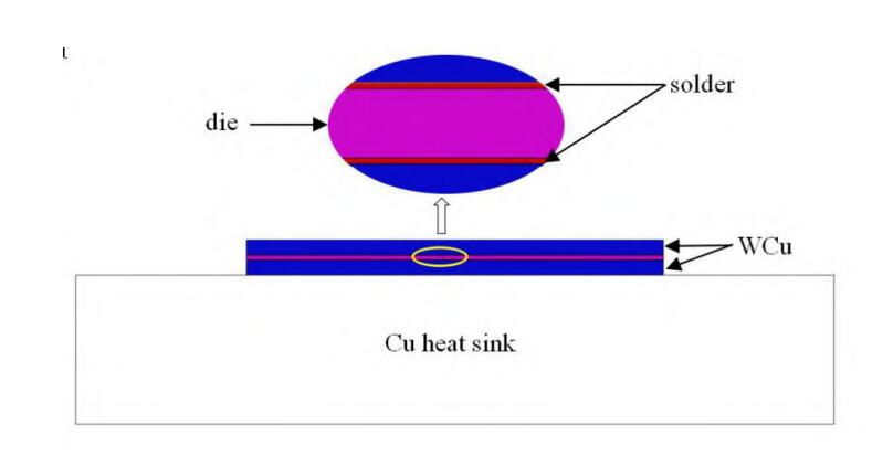
The simulation structure in this paper is shown in Figure 1. From bottom to top, it is Cu heat sink, WCu sub-heat sink, solder, laser chip, solder, WCu sub-heat sink. The laser chip is soldered to the heat sink by solder, and the thermal expansion coefficients of the layers in the package structure are not matched, and the temperature change will cause thermal stress and deformation. In order to facilitate the processing, some approximations are used in the simulation: (1) the complex laser die structure is equivalent to a layer of GaAs material; (2) the relevant thermal parameters such as the thermal expansion coefficient of each layer of material do not change with temperature; Only consider the thermal stress caused by the temperature change, and when the temperature is higher than the melting point of the solder, the laser die has no stress; (4) ignore the influence of factors such as phase change.
![]()
![]()
![]()
![]()

Fig.1. Semiconductor laser bar package structure
The simulation steps based on COMSOL Multiphysics are as follows: Using the model wizard that comes with the software, the spatial dimension is selected as a three-dimensional structure, and the physical field is the thermal stress (including solid mechanics and solid heat transfer) under the structural mechanics module, and the solution type is steady state solution. According to the structure shown in Figure 1, the corresponding geometric models are built in COMSOL Multiphysics, and they are combined into a consortium, and then the materials are added to the geometric model. The relevant material parameters are shown in Table 1. Next, the most critical is the setting of the heat source and boundary conditions, which directly determines the convergence of the model calculation results and the consistency with the real situation. Since the thermal stress analysis module involves both solid mechanics and solid heat transfer, the boundary conditions are set separately. In solid mechanics, the boundary conditions perpendicular to the direction of the die are set to free expansion; the interface of the layers is set to a uniform continuous pair; a point is selected at any vertex of the bottom surface of the Cu heat sink, and a fixed constraint is imposed at this point. In solid heat transfer, the laser die is treated as a heat source with a heat rate of 50 W; the interface of each layer of material is set to the thermal contact boundary condition; the Cu heat sink ground is set to room temperature (20 ° C); Set to convective heat flux boundary conditions, heat convective heat transfer with external air, ambient temperature 20 °C. Then, the model is meshed, and the model is divided into a triangle mesh or a tetrahedral mesh. The finer the meshing, the more accurate the calculation result, and the corresponding computer memory requirements are higher and the calculation time is longer. In this model, the laser die temperature and thermal stress distribution are mainly analyzed. In order to make the calculation result more accurate, the die and solder mesh are extremely refined; in order to improve the calculation speed and save computer memory, The meshing of the WCu heat sink and the Cu heat sink is roughened. Finally, the model is calculated and the calculation results are visualized.
![]()
![]()
![]()
![]()
- Results analysis and discussion
3.1Different solders
At present, in the package of high-power semiconductor laser bars, the widely used solders mainly include In solder and AuSn solder. In solder is a soft solder [12], which has good plastic deformation characteristics and low stress, but in high temperature environment, it tends to cause the growth of weld whiskers, accelerate the thermal fatigue of the weld layer, and cause serious electromigration, resulting in laser The diode failed early. AuSn solder is a hard solder [13], which has excellent fatigue and creep resistance, high yield strength, good thermal conductivity, no flux, and no serious electromigration. However, since the gold-tin solder is a hard solder, the ductility is poor, and the sintering process introduces excessive stress, so the welding process is more demanding. This paper first simulates the high-power semiconductor laser strips of In solder and AuSn solder package, and analyzes the temperature and thermal stress distribution during operation. In the simulation, the size of the Cu heat sink is 20000×20000×4000μm, the size of the WCu heat sink is 11000×2000×400μm, the size of the In and AuSn solder is 11000×2000×10μm, and the size of the laser chip is 11000×2000× 120 μm.
![]()
![]()
![]()
![]()
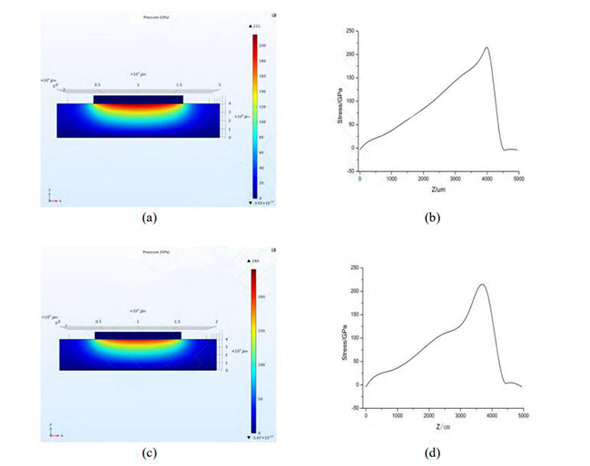
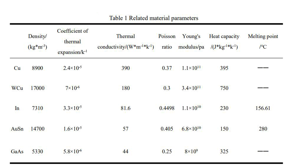
Fig.2. Nephogram of thermal stress distribution of laser chips with different solder packages and stress distribution on the central axis of the end face:
- In solder, thermal stress nephogram (b) In solder, stress distribution on the axis of end face
![]()
![]()
![]()
![]()
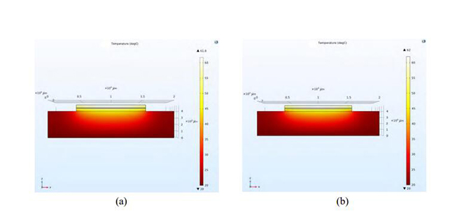
Fig.3. Temperature distribution of laser with different solder packages:
- In solder (b) AuSn solder
The simulation results are shown in Fig. 2 and Fig. 3. As can be seen from Fig. 2(a) and Fig. 2(c), the maximum thermal stress of the high power semiconductor laser of both In solder and AuSn solder package is generated with Cu heat. The interface between sink and WCu has values of 215GPa and 240GPa, respectively. Figure 2(b) and Figure 2(d) show the stress distribution on the central axis of the end face of the structure. The thermal stress of the laser die of the In solder and AuSn solder package is 3.57GPa and 3.83GPa, respectively. Figure 3 shows the temperature distribution of the package structure. As can be seen from the figure, the maximum temperature is generated in the laser die portion. The maximum temperature of the laser chip in the In solder and AuSn solder package is 61.8 ° C and 62 ° C, respectively. The analysis is as follows. It can be seen from Table 1 that the thermal expansion coefficient of the laser die is 5.8×10 -6 k -1 , and the thermal expansion coefficients of the In solder and the AuSn solder are 3.3×10 -5k -1 and 1.6×10 -5k -1 , respectively. Compared with AuSn solder, the thermal expansion coefficient of In solder matches the thermal expansion coefficient of laser die, and In solder is soft solder, part of the stress generated by laser chip can be released, and AuSn solder is hard solder, stress can not be released. Therefore, the laser dies of the AuSn solder package are subject to greater thermal stress [14]. At the same time, the temperature of the In solder is higher than that of the AuSn solder, and the heat dissipation of the overall structure is better, so the temperature of the laser die of the In solder package is lower. In order to verify the correctness of the simulation results, according to the structure shown in Figure 1, 808nm high-power semiconductor laser bars were encapsulated with In solder and AuSn solder, respectively, and their spectral distributions were measured, as shown in Figure 4. Figure 4(a) shows the laser spectral distribution image of the In solder package, and Figure 4(b) shows the laser spectral distribution image of the AuSn solder package with peaks of 800.5 nm and 798 nm, respectively. Nm, compared to In solder, the AuSn solder packaged laser die is subject to greater thermal stress and greater wavelength blue shift.
![]()
![]()
![]()
![]()
Fig.4. Laser spectrum distribution in different solder packages: (a) In solder (b) AuSn solder
3.2 Different thickness solder
It can be seen from Table 1 that whether it is In solder or AuSn solder, the parameters such as thermal expansion coefficient, thermal conductivity and Young’s modulus are quite different from those of laser die and WCu heat sink. The thickness of solder will be the same for laser tube. Core temperature and thermal stress distribution have an important impact. For this reason, thermal stress simulations of high-power semiconductor laser bars with different thickness solder packages are performed. At present, the thickness of the AuSn solder used in the high-power semiconductor laser bar package is about 10 μm in actual production, so the thickness of the AuSn solder used in the simulation is 5 μm, 10 μm, 15 μm, 20 μm, respectively. The effect of die temperature and thermal stress distribution. The dimensions of the Cu heat sink, WCu heat sink, and laser chip in the simulation are all consistent with those in Section 3.1. Figure 5 shows the maximum thermal stress and temperature of the laser die as a function of solder thickness. As can be seen from the figure, as the thickness of the AuSn solder increases, the thermal stress and temperature of the laser die tend to increase. Here, considering the thermal expansion coefficient matching and thermal conductivity: the thermal expansion coefficient of the AuSn solder is different from the thermal expansion coefficient of the laser die, so that the thermal stress inside the laser die will generate a large thermal stress; The thermal conductivity of AuSn solder is low. As the thickness of the solder increases, the heat generated by the laser die is more difficult to release, resulting in an increase in the temperature of the die and an increase in thermal stress, which creates a vicious cycle that may eventually cause the die to rupture. It can be seen from the simulation results that the smaller the thickness of the solder, the lower the thermal stress and temperature inside the laser die, but this is not the case in practical applications. If the solder thickness is too thin, it may cause the laser die to be soldered poorly or the solder may be unevenly distributed. If the laser is not soldered tightly, it may cause cracking between the die and the WCu secondary heat sink. If there is a cavity inside the solder layer, it will cause local hot spot effect, which seriously affects the stability and life of the device. Therefore, the determination of the thickness of the solder layer is determined by a combination of factors and needs further optimization.
![]()
![]()
![]()
![]()
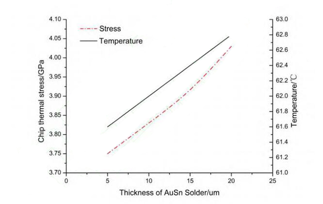
Fig.5. Thermal stress and temperature maximum Distribution of laser chips packaged with AuSn solder of different Thicknesses
3.3 Different thickness
In order to compensate for the mismatch between the thermal expansion coefficient of the laser die and the Cu heat sink, the WCu sub-heat sink often uses the WCu sub-heat sink as the transition heat sink in the package of the high-power semiconductor laser bar, which can effectively alleviate the thermal stress of the laser die. The big problem is to protect the die. However, compared with the Cu heat sink, the thermal conductivity of the WCu heat sink is poor. If the thickness is too large, it will adversely affect the heat dissipation of the laser chip. If the thickness is too small, the thermal stress will not be relieved. This section analyzes the effects of different thickness WCu heat sinks on laser die temperature and thermal stress distribution. At present, the thickness of the WCu sub-heat sink used in the high-power semiconductor laser bar package is about 400 μm in actual production, so the thickness of the WCu sub-heat sink used in the simulation is 300 μm, 350 μm, 400 μm, 450 μm, 500 μm, respectively. The dimensions of the Cu heat sink, AuSn solder, and laser chip in the simulation are all the same in Section 3.1. The thermal stress and temperature of the laser die change with the thickness of the WCu secondary heat sink as shown in Figure 6.
![]()
![]()
![]()
![]()
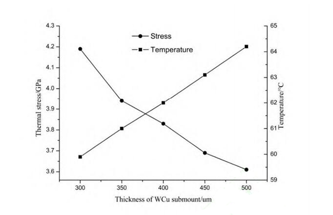
Fig.6. Distribution of maximum thermal stress and temperature in laser chip packaged with different thickness WCu secondary heat sink
As can be seen from the figure, when the thickness of the WCu sub-heat sink increases from 300μm to 500μm, the thermal stress of the laser die decreases from 4.19GPa to 3.61GPa, and the maximum die temperature rises from 59.9°C to 64.2°C. Compared with the Cu heat sink, the thermal expansion coefficient of the WCu sub-heat sink is closer to the thermal expansion coefficient of the laser die. Therefore, as the thickness of the WCu sub-heat sink increases, the thermal stress of the chip is reduced by the Cu heat sink. However, since the thermal conductivity of the WCu sub-heat sink is inferior to that of the Cu heat sink, the increase in the thickness of the WCu sub-heat sink will result in an increase in the overall thermal resistance of the device, poor heat dissipation, and an increase in the temperature of the laser die. It can be seen from Figure 6 that considering the thermal stress and temperature distribution of the laser die, the thickness of the optimal WCu sub-heat sink is 380 μm.
- Summary
Packaging is critical in high-power semiconductor laser applications, and the quality of the package determines the stability and lifetime of the laser. Based on the actual high-power semiconductor laser device, this paper uses the multiphysics simulation software COMSOL Multiphysics to simulate the high-power semiconductor laser strips of different solders, different thickness solders and different thicknesses of tungsten-copper sub-heat sink packages, and measured different The “Smile” value of the laser bar under the package condition. The results show that the thermal stress maximum is generated at the interface between the WCu sub-heat sink and the Cu heat sink, whether it is In solder or gold tin solder; the thermal stress of the laser die of the same thickness In solder and AuSn solder package is 3.57GPa and 3.83, respectively. GPa, the maximum temperature of the die is 61.8 ° C and 62 ° C, respectively, the spectral peaks are 800.5 nm and 798 nm; reducing the thickness of the solder, which is beneficial to reduce the thermal stress and temperature inside the laser die, but the thickness of the solder is too thin, then It may lead to poor soldering of the laser die or uneven solder distribution, and voids inside the solder layer. Therefore, the thickness of the solder should be selected as a whole. As the thickness of the WCu sub-heat sink increases, the laser die is subjected to thermal stress. Small, but the die temperature has increased, the optimal tungsten copper secondary heat sink thickness is 380μm. This paper provides a basis for optimizing the design of high-power semiconductor laser strips, and has guiding significance for actual production.